

Intel has released their first mobile processors based on their highly anticipated Meteor Lake platform, the Core Ultra H and the Core Ultra U series. Available today, the Ultra Core H series has four SKUs, including two Ultra 7 16 core (6P+8E+2LP) chips and two 14 core (4P+8E+2LP) Ultra 5 chips. All run at a base TDP of 28 W, with a maximum turbo TDP of up to 115 W. The Core Ultra-H series is designed for ultra-portable notebooks but offers more performance in both computing and graphics within a slimline package.
Also announced is the Intel Core Ultra U-series, which includes four 15/57 W (base/turbo) SKUs, with two Core Ultra 7 and two Core Ultra 5 SKUs, and all coming with a variance in P, E-core and Intel’s latest integrated Arc Xe graphics frequencies. All of Intel’s announced Core Ultra U-series processors for mobile feature 10 CPU cores, with two Performance cores and eight Efficiency cores, making them ideal for lower-powered and ultra-thin notebooks.
The launch of Intel’s tile-based Meteor Lake SoC marks the first step in a series of power-efficient and AI-focused chips on Intel 4 for the mobile market, which is ultimately designed to cater to the growing need to utilize AI inferencing on-chip. Both the Intel Core Ultra H and U families of chips include two new Low Power Island (LP-E) cores for low intensity workloads, with two Neural Compute Engines within the Intel AI NPU designed to tackle generative AI inferencing.
Intel Core Ultra Processors: Quickly Recapping Meteor Lake
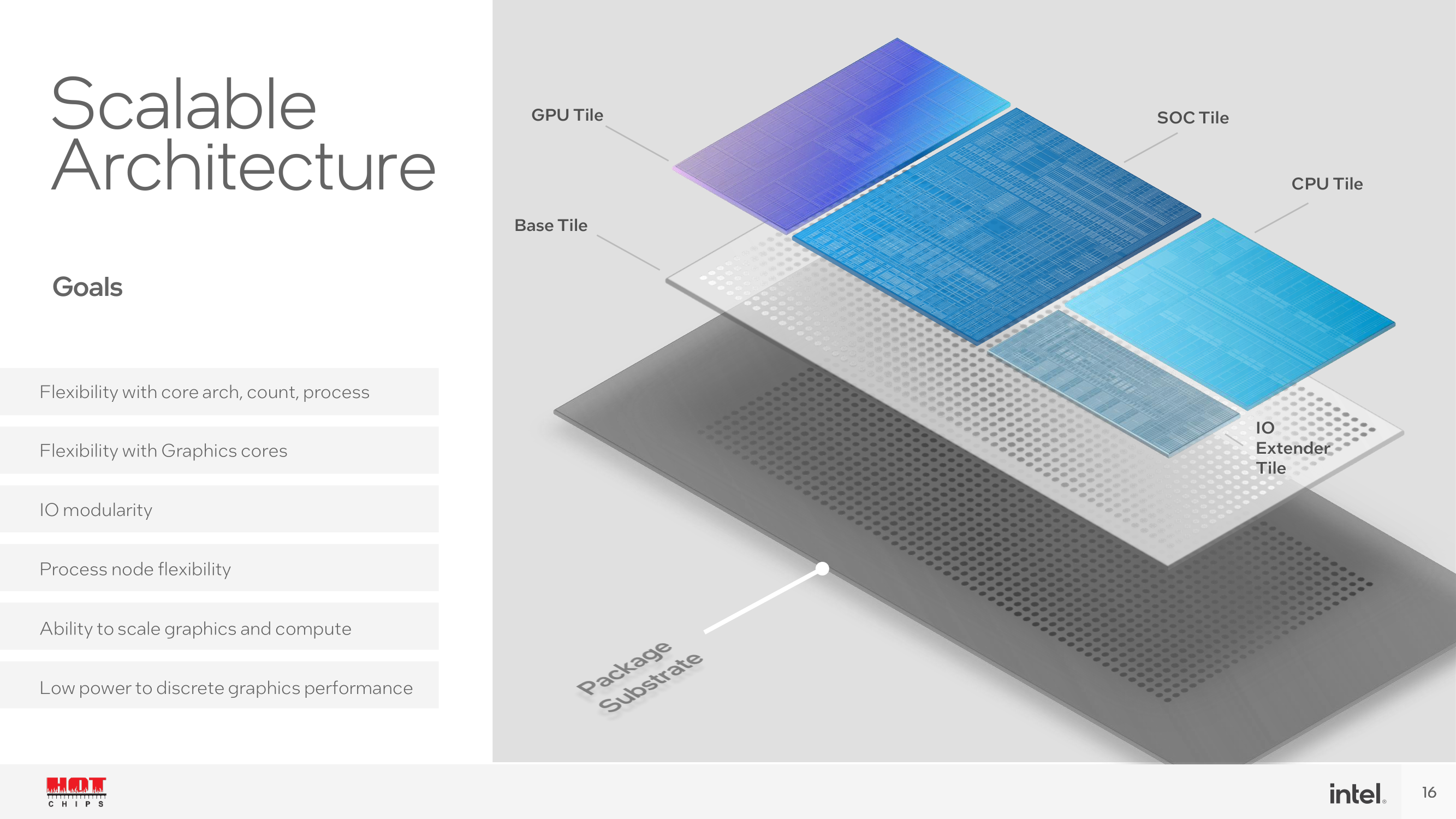
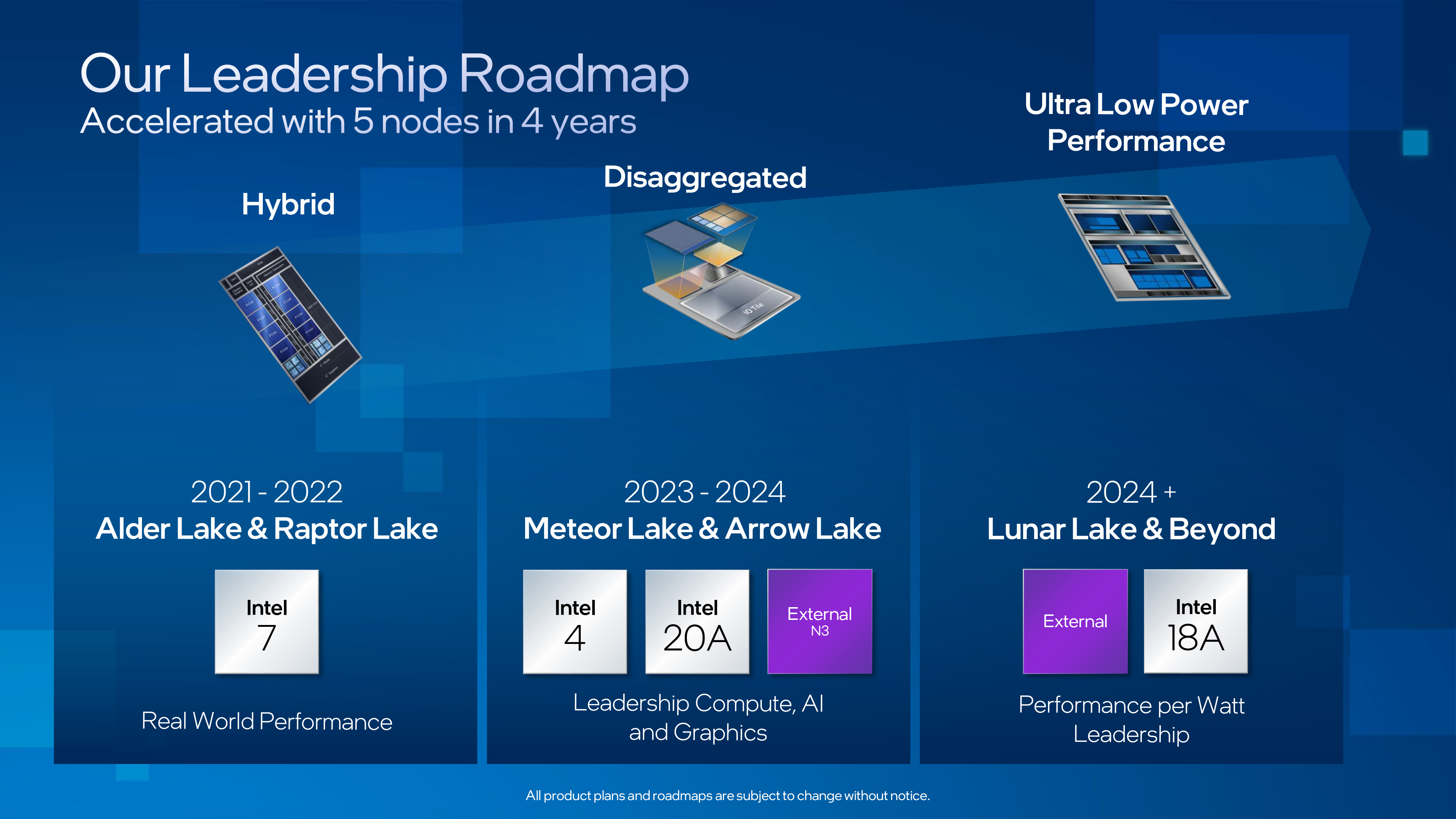
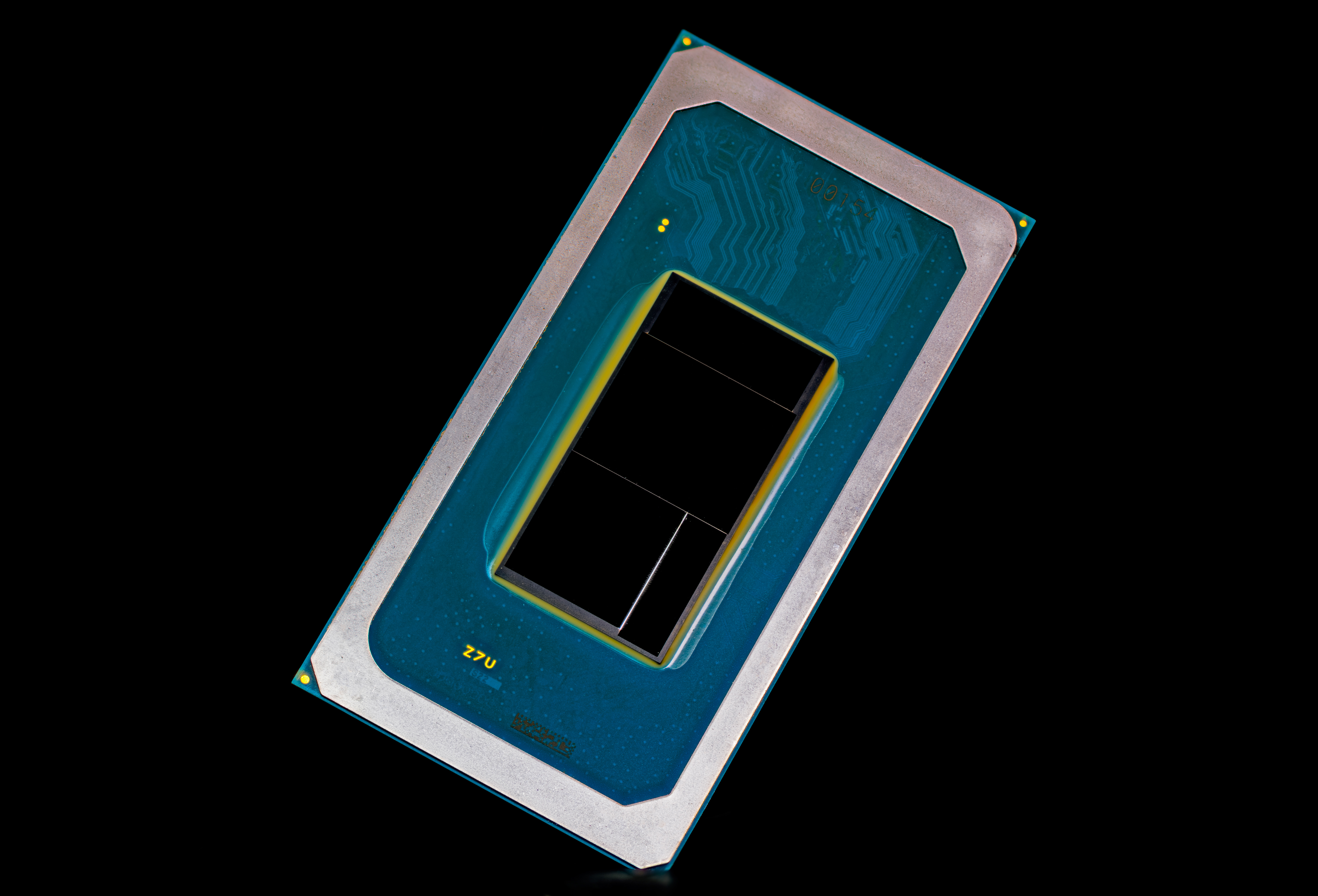
In September, Intel unveiled their chiplet-based Meteor SoC architecture during their annual Innovation event, which slices things up from a conventional monolithic processor into four individual tiles. Created using their Foveros 3D packaging, Intel is using a mix of process nodes to put together their first chiplet-based CPU. The most critical chiplet, the CPU tile, is being built on Intel’s EUV-based Intel 4 node, the latest and greatest fab tech out of the company, and which promises to provide robust gains in performance and energy efficiency compared to the long-standing Intel 7 process. Joining the CPU tile are tiles for the integrated GPU, SoC, and I/O functions, which are built on a mix of trailing-edge and even external process nodes.
Below is our deep dive into Meteor Lake as an SoC architecture, as well as all the key components such as the compute, I/O, graphics, and SoC tile:
Quickly recapping the Meteor Lake SoC architecture, it is essentially four interconnected tiles, including a compute, graphics, SoC, and an I/O tile. Within each of the tiles are a host of new advancements, including the Redwood Cove Performance (P) cores and Crestmont Efficiency (E) cores housed within the compute tile. On top of this, Intel also has a special variant of the E-core, called the Low Power Island or LP-E core, which is integrated into the SoC tile and is designed to tackle low-intensity workloads. Notably, because the SoC tile is essentially always active, the LP-E core is very cheap to use from an energy standpoint compared to powering up the CPU tile.
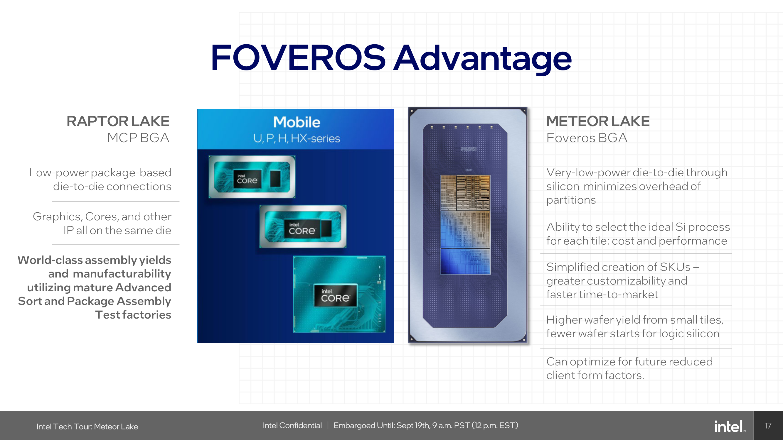
Meteor Lake is an upgrade and a significant architectural shift for Intel, moving away from traditional monolithic designs to a chiplet-based approach. This shift, leveraging Intel’s Foveros 3D packaging technology, introduces 3D chip stacking to overcome the limitations of 2D chip layouts. Like other shifts we’ve seen towards using chiplets, the architecture’s focus on disaggregation, power efficiency, and flexible silicon gives Intel new options for assembling CPUs out of individual blocks.
The architecture’s modular design facilitates scalable power management, which can be optimized, allowing each tile to operate independently, thereby maximizing performance and energy efficiency. This disaggregation also enables Intel to use different silicon processes for each tile, offering flexibility and cost savings in manufacturing. Meteor Lake’s use of Foveros packaging and low-power, low-distance die-to-die interconnects marks a departure from the Multi-Chip Packaging (MCP) used in the previous Raptor Lake mobile chips, allowing for more optimized power usage and chip customization.
Offering four differently built yet highly functional tiles, Intel’s Meteor Lake looks to increase customizations of their notebook SKUs in the future. Offering a tile solution enables Intel to amalgamate a variety of different engines, blocks, and tiles into one chip. Using their Foveros packaging technology also allows Intel to build chips differently, and more importantly, it means they aren’t limited to one specific manufacturing process – a hedge against problems with any one fab/node. Even in the present Core Ultra U and H series chips Intel is announcing today, the manufacturing choice for each of the tiles differs slightly, with the compute tile built on Intel 4 node, the graphics tile with Arc Xe graphics is built on TSMC’s N5 node, and the SoC and I/O tiles are built using TSMC’s N6 process. This flexibility means Intel can implement new technologies from different process nodes, tapping the benefits of any given node’s specialty (e.g. frequency or density) and not having to produce (and yield) an entire chip on a leading-edge process.
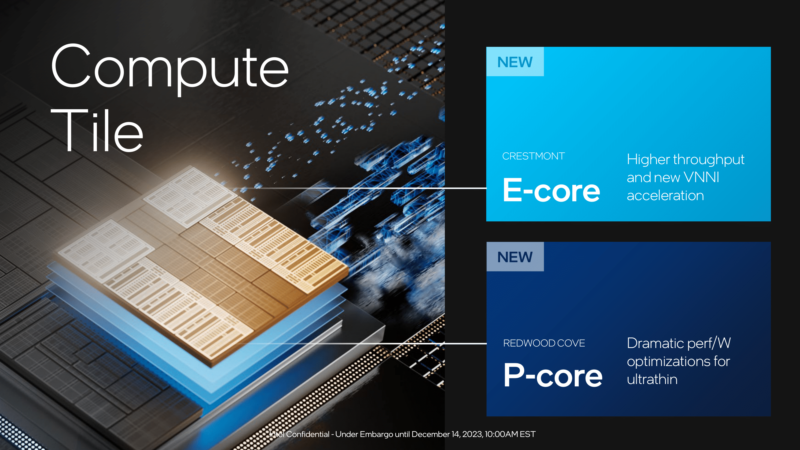
Taking a quick look at the underlying architecture, on the compute tile of the Ultra Core series in the first iteration of Meteor Lake, Intel is using two new CPU architectures within the heterogeneous design. Intel’s Meteor Lake compute tile is built using the Intel 4 node, and the process offers 2x the area scaling for the high-performance logic libraries compared to the previous Intel 7 node. The latest Performance cores are called Redwood Cove, which Intel claims brings new benefits over the previous Golden Cove P-core, including better per-watt performance efficiency, improved feedback through Intel Thread Director within Windows 11, more bandwidth, and improved performance monitoring capabilities. All of these improvements combined are designed to provide enhanced feedback to Thread Director to help optimize core performance and direct workloads to the right cores.
Notably, however, Intel hasn’t said anything about Redwood Cove’s IPC. Reading between the lines, we are left with the distinct impression that Redwood Cove’s IPC is similar (if not identical to) Golden Cove’s. And if that’s the case, it means Intel won’t be moving the needle on single threaded performance in this generation – at least, not in TDP-unconstrained scenarios. In fact, the peak P-core clockspeeds for Core Ultra (Meteor Lake) chips are lower than 13th Gen Core Mobile (Raptor Lake) chips – 5.1GHz vs. 5.4GHz – so it’s entirely plausible that some Core Ultra chips could lose in single-threaded CPU benchmarks to 13th Gen Core chips. All of which is to say that while Intel should still pick up some real-world performance here due to the energy efficiency improvements, Redwood Cove is more of a side-grade in terms of architecture.
Intel’s efficiency cores, on the other hand, should deliver a major improvement. Intel is using their Crestmont cores for the efficiency cores, which Intel claims bring IPC gains over their 13th Gen Raptor Lake E-cores, as well as AI acceleration optimizations in VNNI and ISA, as well as enhanced feedback to Intel Thread Director. For low-intensive workloads, Intel includes two new Low Power Island (LP-E) cores on each of the announced SKUs housed within the SoC tile and allows light workloads to be offloaded onto these cores to enhance overall power efficiency. Intel Thread Director with Windows 11 is a key component in ensuring the right workloads go onto the right cores for the best performance and power efficiency levels.
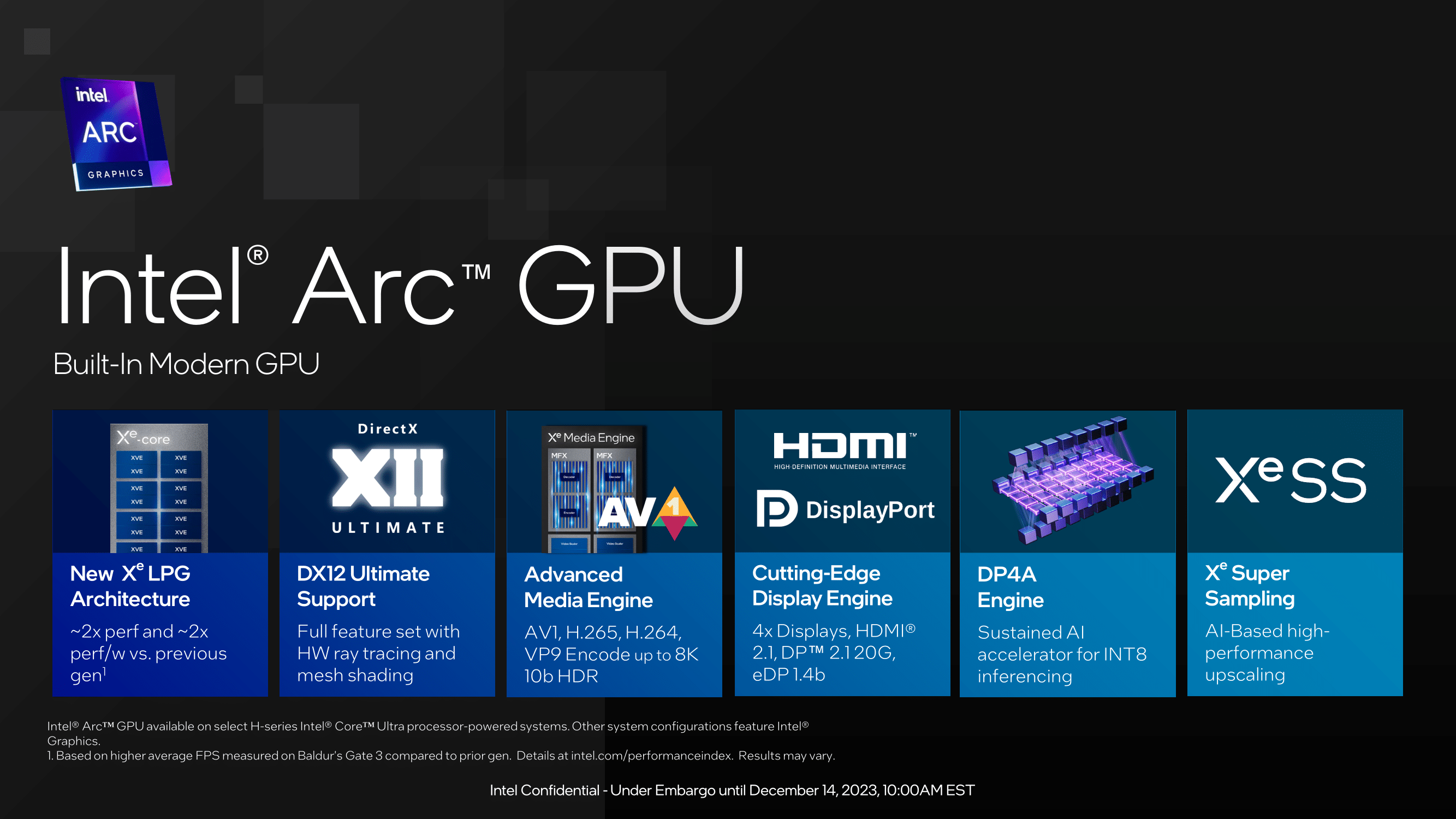
Another key component (or tile) within the heterogeneous Meteor Lake SoC design is an upgrade to Intel’s Arc graphics architecture. Built on TSMC’s N5 node, the graphics core of choice is the Arc Xe-LPG core, which is a derivative of Intel’s discrete Xe-HPG GPU architecture. The GPU tile is comprised of 16 Vector Engines with a 256-bit bus width and 192 KB of shared L1 cache per core. Each Vector Engine can perform 16 FP32 and 32 FP16 operations per clock, along with a shared FP64 execution port capable of 64 INT8 operations per clock. Also featured is a dedicated FP64 unit, which is new compared to Raptor Lake (13th Gen) and has pairs of vector engines operating in lockstep for improved efficiency. Notably, this architecture does not include Intel’s matrix engines (XMX), so while Intel can run AI tasks on the GPU, it doesn’t have quite the same punch as on their desktop hardware.
For Meteor Lake, Intel has opted to disaggregate the Xe Media Engine from the graphics tile and implanted it within the SoC tile, which is built on TSMC’s N6 node. The Xe Media Engine includes two multi-format codecs (MFX), which are designed to encode and decode but do so off of the GPU to improve power efficiency. Meteor Lake supports a wide variety of codecs, including AV1, HEVC, AVC, and VP9, with capabilities including up to 8K60 HDR decoding. The Xe Media Engine is also equipped to handle up to 8K 10-bit and HDR encoding.
Launching Softly: Limited Hardware and No Reviews
Despite today being the official launch of the Core Ultra series and Meteor Lake platform, you won’t find any reviews for the hardware. And we’re not sure you’ll be able to find much hardware, either.
In a significant departure from how Intel has handled previous mobile-first architecture launches, the company has not sampled any laptops to the press for review ahead of today’s launch. So while you can go out and buy a Core Ultra laptop today (in theory, at least), we can’t actually show you how it performs, or even validate Intel’s own performance claims.
Looking at the bigger picture, there are multiple signs that Intel is struggling to get Meteor Lake out the door for a 2023 launch, which they’ve long promised since it was added to their public roadmap in 2021. The company is still trying to recover from their multiple fab delays in the 10nm/7nm era, and the chip delays that came with that. Meteor Lake is Intel’s first major client processor built with an EUV process (Intel 4), and delivering it on time would be an important sign that Intel has put their fab and chip development processes back on track.
Still, the lack of review hardware, combined with the fact that the flagship Core Ultra 9 185H SKU won’t even be available until Q1, gives us pause. If Meteor Lake is indeed launching in 2023, then it’s only by the skin of Intel’s teeth: 2 weeks before the end of the year, and what we strongly suspect will be a very limited number of laptops available at retail for today’s launch.
Which is not to kick Intel while they’re still trying to pick themselves back up. But if Intel hadn’t already promised a 2023 launch for Meteor Lake, then this would almost certainly would have been a CES launch, if not later.
In the meantime, all we can do for now is talk about specifications and performance expectations. Whether or not Meteor Lake technically launches in 2023, it’s going to be a 2024 product, and that goes for everything from reviews to wide hardware availability.
The Intel Core Ultra H-Series: Up to 115 W of Mobile Performance for Notebooks
With the launch of Intel’s Core Ultra H and U-series, these are the first chips to feature Intel’s new processor branding. As part of the most significant brand change from Intel in the last 15 years, the Core Ultra 9, 7, and 5 series is designed to split their client chips into easily denote categories, with the Ultra naming reserved for their premium parts. The biggest change is that Intel is dropping the ‘i’ prefix, which is perhaps one of their most denominable processor identities over the last 15 years, e.g., the Core i5.
Intel is launching four SKUs under their Core Ultra branding for the H-series, covering the Ultra 7 and Ultra 5 segments. The flagship Ultra 9 chips, on the other hand, will remain missing in action for another quarter – the Core Ultra 9185H isn’t expected to launch until sometime in Q1 2024. It’s worth highlighting Intel’s message here, which seems to be mixed. Typically, the U-series SKUs are reserved for ultrathin notebooks and ultraportables, whereas Intel’s message looks to highlight that the H-series could be used in thinner notebooks too. This remains to be seen, and we’ll find out soon enough when OEMs and vendors start announcing models encompassing Meteor Lake.
Opening with a look and dissection of the specifications on the chips available now, the Core Ultra 7 165H and Core Ultra 7 155H are 16C/22T parts. With six performance (P) cores and eight efficiency (E) cores, adding in the two LP-E cores on the SoC tile brings us to a total of 16 CPU cores that can execute up to 22 threads at once. The Core Ultra 7 165H has a P-core turbo frequency of up to 5.0 GHz with an E-core turbo frequency of up to 3.8 GHz. This also includes 8 Intel Arc Xe cores for the integrated graphics, which can hit to 2.3 GHz and 24 MB of Intel Smart L3 cache.
The Intel Core Ultra 7 155H is slightly slower than the Core Ultra 7 165H, with a 5.0 GHz P-Core turbo and a 2.25 GHz integrated graphics frequency. The new Crestmont E-cores can hit a maximum of 3.8 GHz, while the Core Ultra 7 155H also has 24 MB of L3 cache. The only difference between the two Core Ultra 7 SKUs is a 100 MHz dip in the P-core turbo and a slight 50 MHz dip in graphics clock speed.
Both chips operate with a fairly wide TDP range. The base TDP of the Ultra 7 (and Ultra 5) H-series parts is just 28 Watts, while the entire lineup can turbo at either 64 Watts, or for the fastest devices, 115 Watts. And since we’re talking about mobile parts, do keep in mind that device vendors have a lot of latitude here for further adjusting TDP limits to fit the power and cooling constraints of their devices.
It’s worth highlighting that Intel is comparing a lot of the Core Ultra H-series up against the previous 13th Gen Raptor Lake-Based P-SKUs (28/64 W) when it comes to performance, rather than the the 13th Gen H-series parts. Coming from the previous generations, the base TDP for the H-series has been reduced, from 45 W down to 28 W. In practice, Intel has seemingly collapsed the P and H series (which were already using the same silicon and packages) down to a single line, the H-series, for the first generation of Core Ultra.
| Intel Core Ultra H-Series Processors: Meteor Lake (Intel 4) | ||||||||
| AnandTech | Cores (P+E+LP/T) |
P-Core Turbo Freq |
E-Core Turbo Freq |
GPU | GPU Freq | L3 Cache (MB) |
Base TDP | Turbo TDP |
| Ultra 9 | ||||||||
| Core Ultra 9 185H* | 6+8+2/22 | 5100 | 3800 | Arc Xe (8) | 2350 | 24 | 45 W | 115 W |
| Ultra 7 | ||||||||
| Core Ultra 7 165H | 6+8+2/22 | 5000 | 3800 | Arc Xe (8) |
2300 | 24 | 28 W | 64/115 W |
| Core Ultra 7 155H | 6+8+2/22 | 4800 | 3800 | Arc (8) | 2250 | 24 | 28 W | 64/115 W |
| Ultra 5 | ||||||||
| Core Ultra 5 135H | 4+8+2/18 | 4600 | 3600 | Arc Xe (7) |
2200 | 18 | 28 W | 64/115 W |
| Core Ultra 5 125H | 4+8+2/18 | 4500 | 3600 | Arc Xe (7) | 2200 | 18 | 28 W | 64/115 W |
*Available from Q1 2024
Note: Intel hasn’t provided us with any base frequency specifications at the time of writing, once we have these, we will update the tables.
Moving down to the Core Ultra 5 series SKUs, like the Core Ultra 7 H-series, there are minor differences in the specifications. The faster of the two, albeit with a 100 MHz faster P-core turbo, is the Core Ultra 5 135H, which is a 14C/18T chip, with 4 P-cores and 8 E-cores making up the compute tile on the two Core Ultra 5 parts. The Core Ultra 5 135H has a 4.6 GHz P-Core turbo with a 3.6 GHz E-core turbo, although there is a slightly lower spec Intel Arc graphics tile with 7 Xe graphics cores that can hit up to 2.2 GHz.
The Core Ultra 5 125H has a 4.5 GHz P-Core turbo, the same 3.6 GHz E-core turbo as the 5 135H, and shares the same Arc integrated graphics clocked up to 2.2 GHz. Both the Intel Core Ultra 5 135H and Core Ultra 5 125H have a base TDP of 28 W, although Intel has provided both a 64 or 115 W turbo TDP specification.
The last of the announced Intel Core Ultra H-series SKUs coincidentally has the highest specs, but it won’t be available until Q1 2024, which is the Core Ultra 9 185H. Like the two Core Ultra 7 chips announced, the Core Ultra 9185 is also a 6P+8E+2LP/22T chip with P-Core turbo clock speeds of up to 5.1 GHz and an E-Core turbo frequency of 3.8 GHz. It has the same Arc-based 8 Xe cores within the graphics tile and is clocked up to 2350 MHz. Unlike the other Core Ultra H-series processors, the Core Ultra 9185 has a higher 45 W base TDP, with a 115 W maximum TDP at turbo clock speeds.
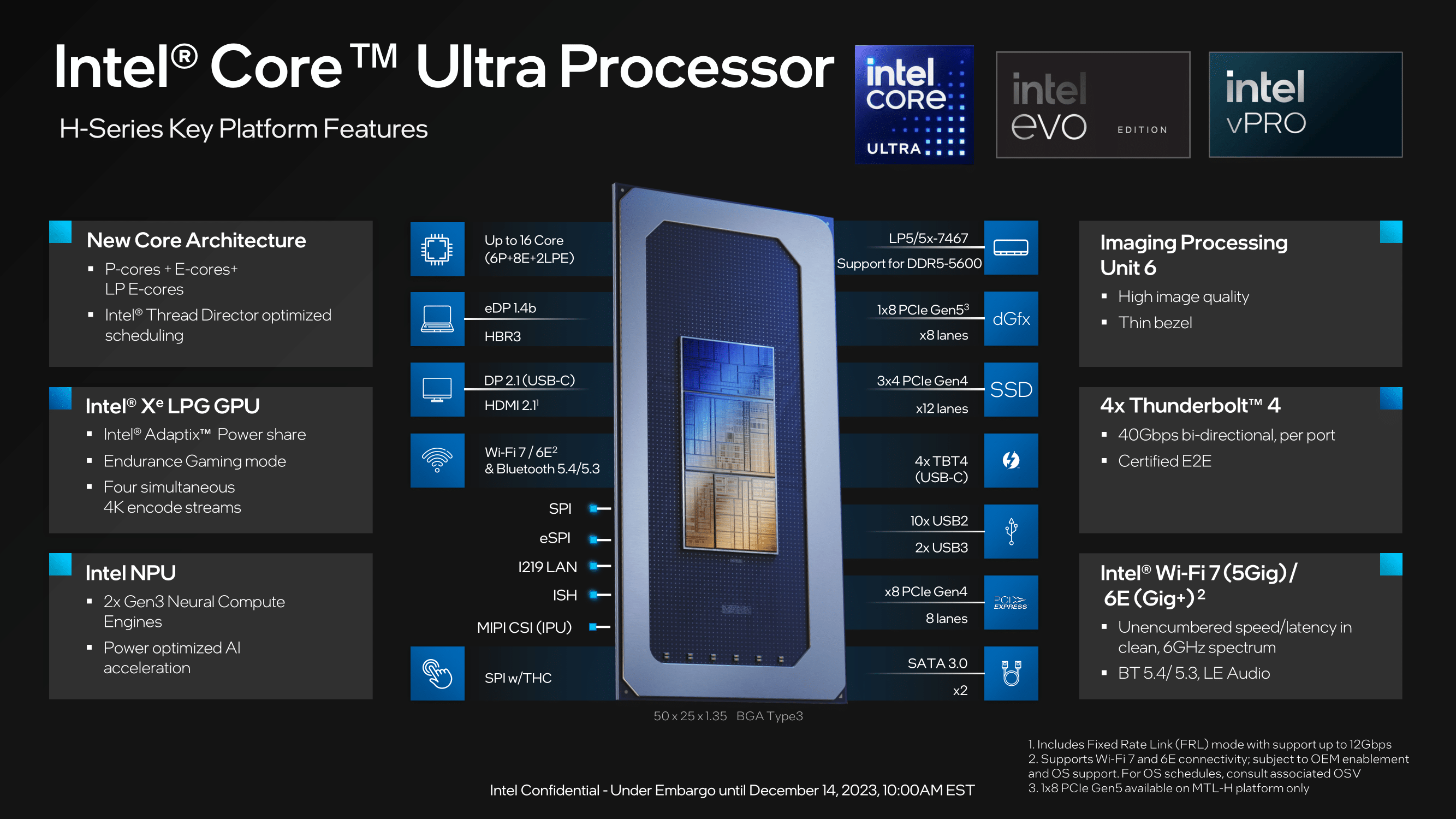
All of the Intel Core Ultra H series SKUs include the aforementioned 2 Low Power Island (LP-E) cores built directly into the SoC tile. They are designed to improve power efficiency by putting low-intensity workloads on the more efficient of the three available core types. Also present within the SoC tile are two Neural Compute Engines, which are Intel’s implementation of an NPU designed for generative AI and are optimized for these types of workloads.
Meanwhile, memory support for the Core Ultra H-series platform includes both DDR5 and LPDDR5(X). The processor is currently validated against DDR5-5600 and LPDDR5X-7467, all attached via a 128-bit memory bus.
For internal I/O, Intel is offering a mix of PCIe 5.0 and PCIe 4.0 lanes on the Core Ultra H-series platform. A single PCIe 5.0 x8 link is available for OEMs looking to include discrete graphics within their models. Meanwhile there are 12 PCIe 4.0 lanes dedicated to driving storage, supporting up to three PCIe 4.0 x4 M.2 SSDs. Finally, another 8 PCIe 4.0 lanes are available for general I/O needs. And for systems that still need additional storage beyond that – particularly of the rotating rust variety, there are a pair of SATA III ports available on the chip.
As for external I/O, the Core Ultra H-series platform includes support for 4x Thunderbolt 4 (USB4) ports, as well as 2x USB 3 and 10x USB 2 ports. The integrated GPU, in turn, can drive DisplayPort 2.1 video out via the Type-C ports, and the silicon supports a dedicated HDMI 2.1 port if an OEM wants to include one.
Finally, on the wireless side of matters, the Meteor Lake platform natively supports Wi-Fi 6E. This is accomplished via the latest generation of Intel’s CNVio technology, which integrates a Wi-Fi MAC in to the host chipset (or this case, the SoC), while the PHY remains a separate module. Integrating it in this fashion keeps down costs (OEMs need only buy the PHY) and makes for a smaller footprint overall.
Intel is also listing Wi-Fi 7 support for Meteor Lake, but it should be noted that this is wholly discrete; there is no native Wi-Fi 7 hardware within the Meteor Lake platform itself OEMs looking to incorporate Wi-Fi 7 would need to include a stand-alone adapter, such as Intel’s BE200. Consequently, we’re expecting to see Wi-Fi 7 support limited to premium notebooks, where OEMs can pass on the higher cost of a discrete adapter and have the space to place it.
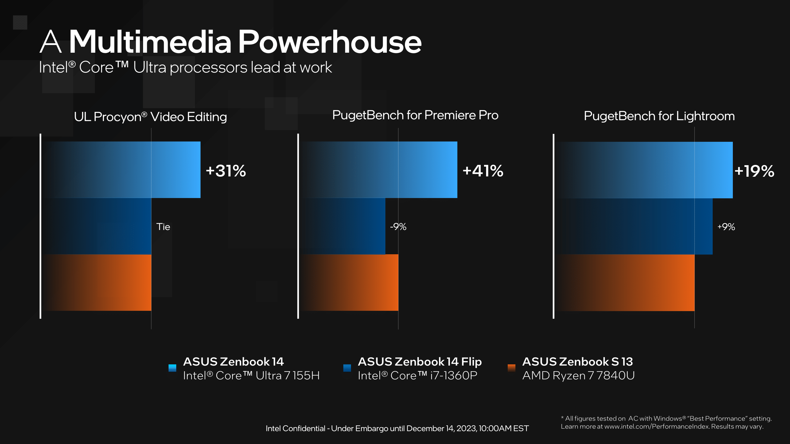
Looking at some of the performance figures Intel provided within their Core Ultra series slide deck, Intel is claiming a performance gain of up to 31% within UL Procyon’s video editing benchmark, with an even larger gain of 41% over the AMD Ryzen 7 7840U processor in PugetBench for Premiere Pro. Using PugetBench for Lightroom, Intel claims the Core Ultra 7 115H is 19% faster in this scenario. While we take vendor and manufacturer’s in-house performance figures with a grain of salt, they still indicate expected performance from new products.
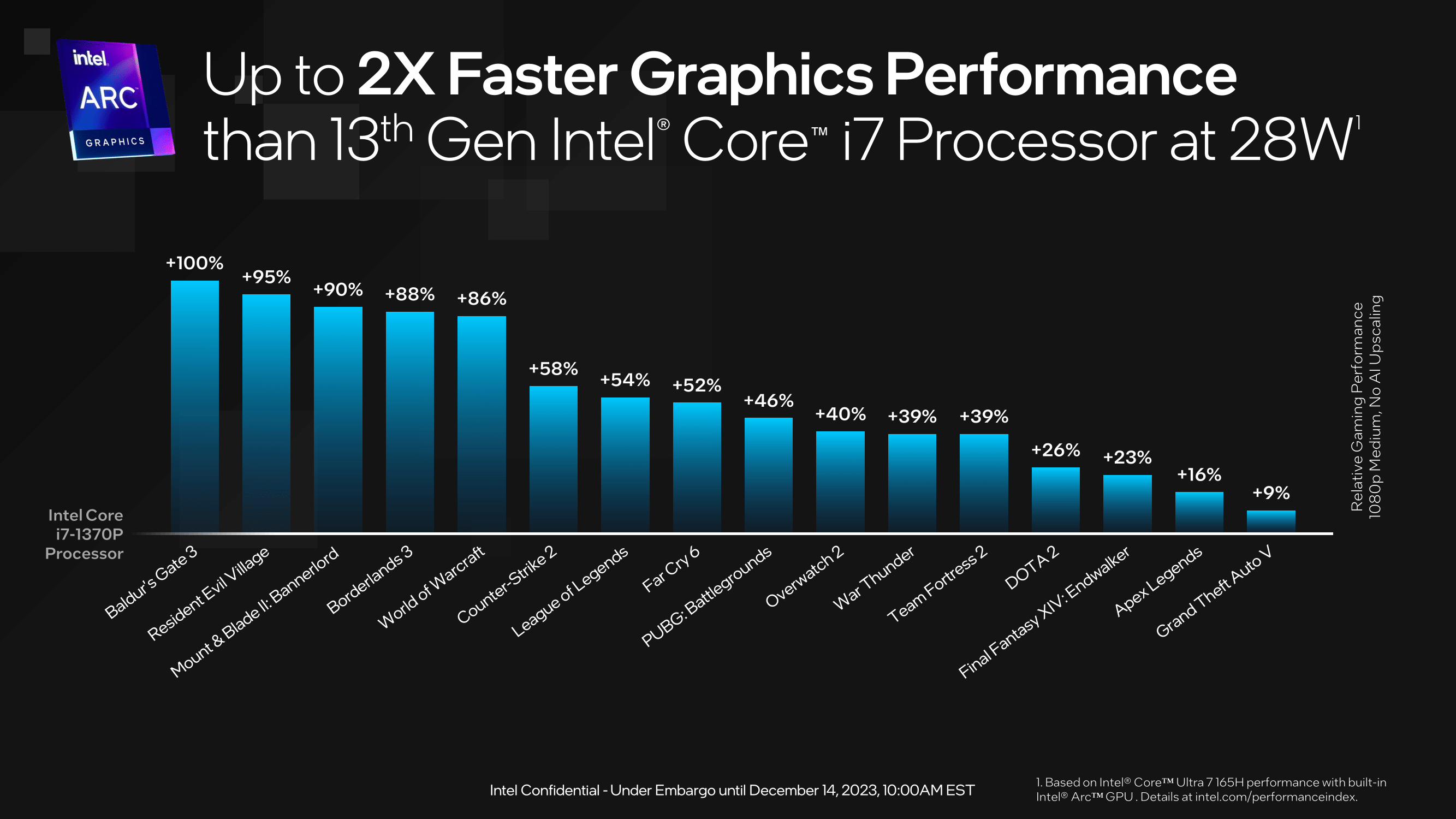
As for GPU performnace, Intel is comparing the latest Arc Xe-LPG integrated graphics on the Core Ultra 7 165H for gaming performance to the previous generation Core i7-1370P. From the in-house testing Intel did, they claim up to 100% gains in Baldur’s Gate 3, with varying levels of performance in other games, such as 88% more FPS in World of Warcraft and 39% in Team Fortress 2. While it’s clear that Intel is pinning a lot of Meteor Lake performance success on the Arc-based integrated graphics, it will be interesting to see how the performance stacks up against discrete options in the coming months.
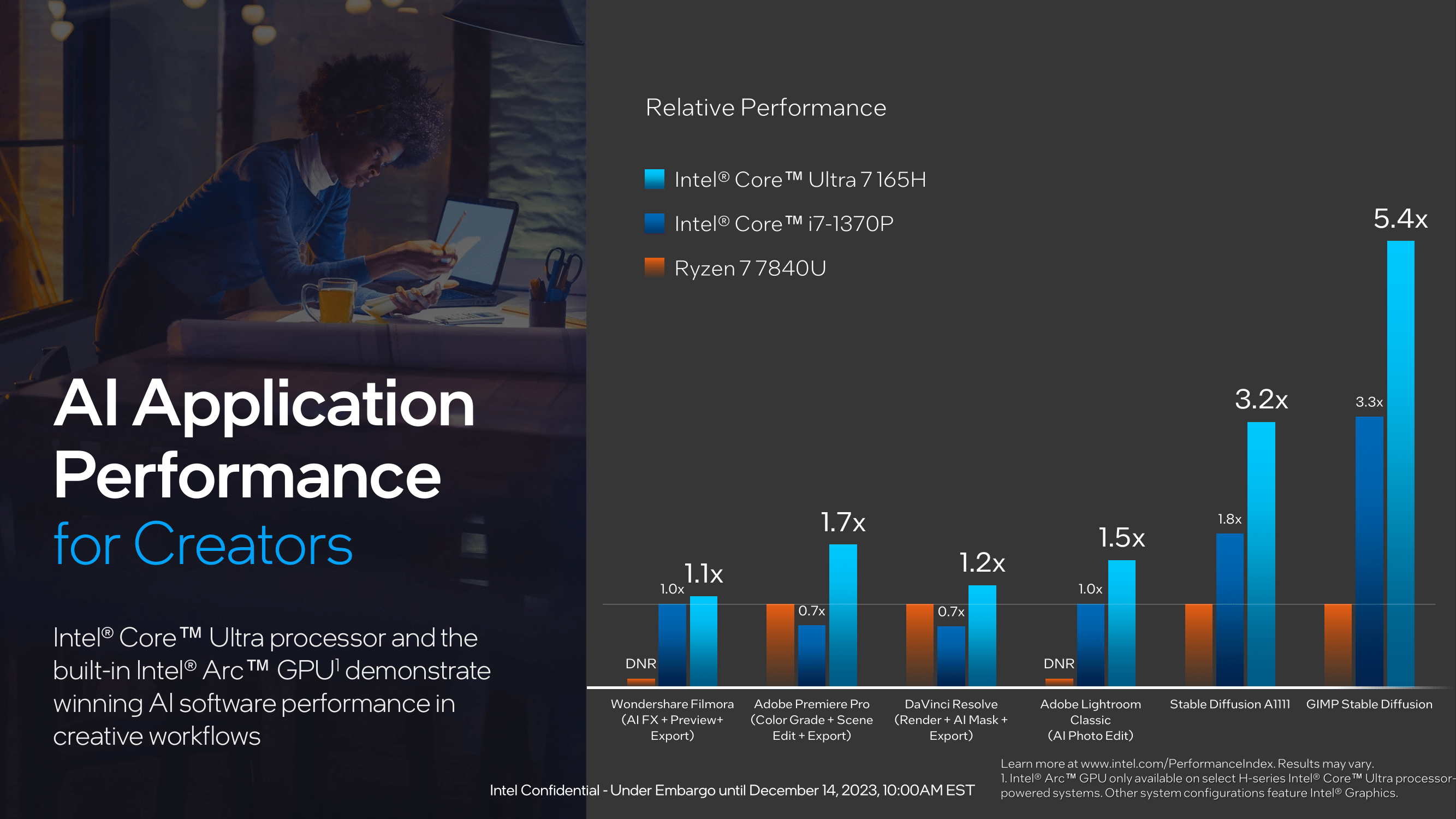
The other metric where Intel is looking to showcase their advantage over the competition is in AI performance. Intel is claiming up to 5.4 X performance in GIMP Stable Diffusion with just the enhanced capabilities from within the Arc Xe-LPG graphics cores over the previous Core i7-1370P and AMD Ryzen 7 7840U processor. Even in applications utilizing generative AI such as Adobe Lightroom, Intel claims up to 1.5 X the performance of the Ryzen 7 7840U.
Again, take vendor/OEM-supplied performance figures with a grain of salt. Still, the performance gains Intel is showing for the Core Ultra H series look impressive on paper, but experiences and figures in the real world may vary.
Intel’s Meteor Lake SoC combines a functional and multi-dimensional approach to AI inferencing, with generative AI across the compute, graphics, and NPU engine block. Intel is creating a clear picture that Meteor Lake has three fully functional AI engines, with the Arc Xe-LPG graphics providing high throughput for AI acceleration for content creation. In contrast, the NPU and its two Neural Compute Engines are designed to offload sustained AI workloads to further enhance power efficiency. The Compute tile itself and the combination of the Redwood Cove (P) and Crestmont (E) cores are designed to handle AI workloads with a lower latency for more precision.
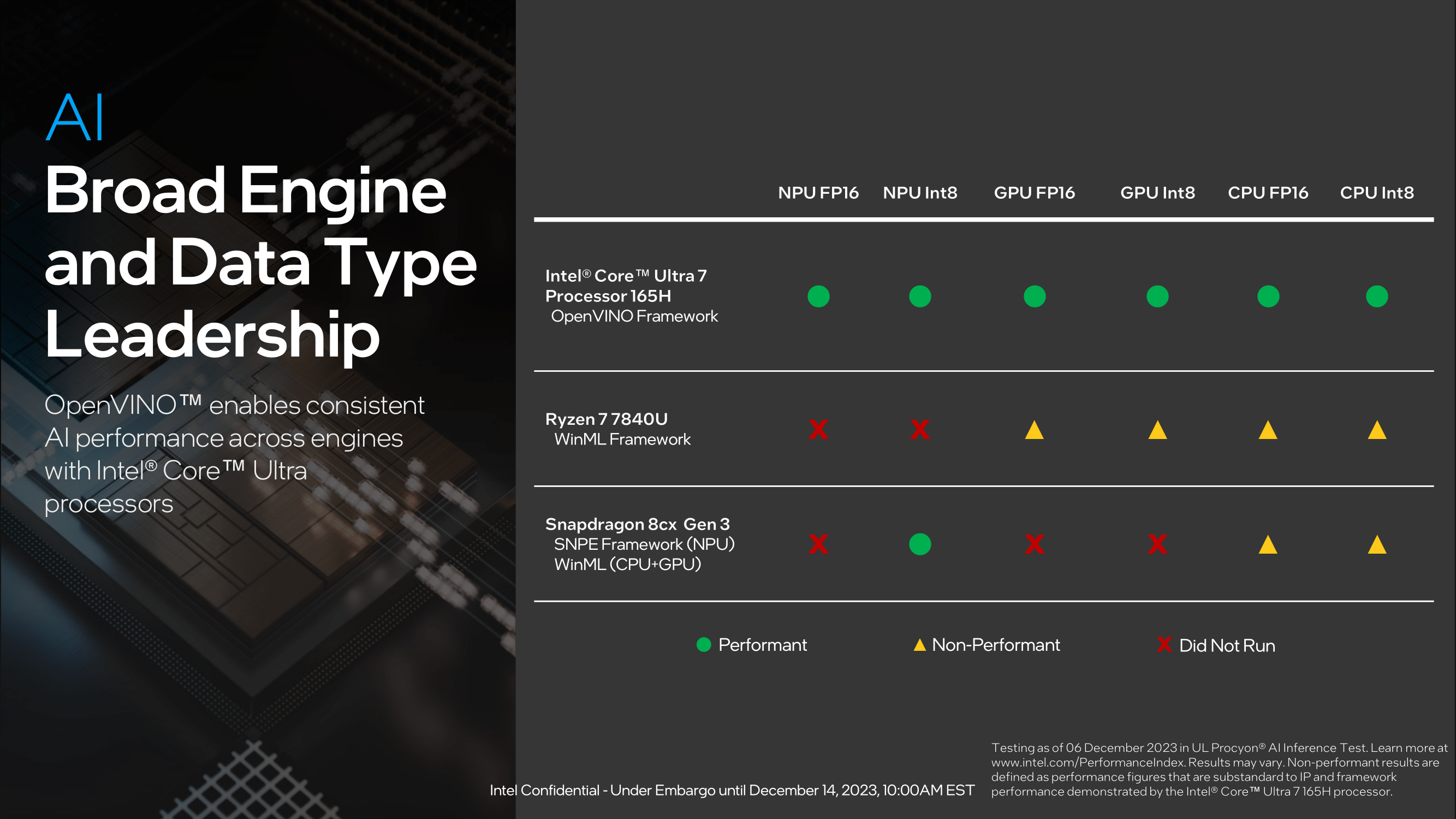
With the PC CPU ecosystem now in a full-on sprint to integrate improved AI/neural network abilities into their designs, we’re also going to see a lot of back-and-forth between vendors on their NPU capabilities and performance in these early days. The newest and most recent part to launch, Intel is quick to tout its support for a large array of numerical formats. Helping matters in Intel’s case, the company is coming into this launch with their already well-developed OpenVINO framework to tap the combined CPU, GPU, and NPU AI capabilities of their hardware.
Intel’s in-house testing in the above chart ran the UL Procyon AI inference benchmark, which is a bit of a messy comparison due to the benchmark’s support for different and vendor-specific backends. Again, experiences and performance may vary.
Intel Core Ultra U-Series: Lower TDPs for Even Thinner and Low Profile Notebooks
Moving onto the new Intel Core Ultra U-series processors, Intel has readied four SKUs available now, while another two are set to be available sometime in Q1 2024.
Starting things off, we have the Intel Core Ultra 7 165U, a 2P+8E+2LP/14T chip with a P-core turbo of up to 4.9 GHz and an E-core turbo frequency of 3.8 GHz. The 7 165U also has 4 Xe integrated graphics cores clocked at 2.0 GHz. The only difference between the Core Ultra 7 165U and the Core Ultra 7 155U is that the 7 155U is slightly slower with a 4.8 GHz P-Core turbo (100 MHz lower) and a 1.95 GHz clocked integrated graphics (50 MHz lower).
| Intel Core Ultra U-Series Processors: Meteor Lake (Intel 4) | ||||||||
| AnandTech | Cores (P+E+LP/T) |
P-Core Turbo Freq |
E-Core Turbo Freq |
GPU | GPU Freq | L3 Cache (MB) |
Base TDP | Turbo TDP |
| Ultra 7 | ||||||||
| Core Ultra 7 165U | 2+8+2/14 | 4900 | 3800 | Arc Xe (4) | 2000 | 12 | 15 W | 57 W |
| Core Ultra 7 164U* | 2+8+2/14 | 4800 | 3800 | Arc Xe (4) | 1800 | 12 | 9 W | 30 W |
| Core Ultra 7 155U | 2+8+2/14 | 4800 | 3800 | Arc Xe (4) | 1950 | 12 | 15 W | 57 W |
| Ultra 5 | ||||||||
| Core Ultra 5 135U | 2+8+2/14 | 4400 | 3600 | Arc Xe (4) | 1900 | 12 | 15 W | 57 W |
| Core Ultra 5 134U* | 2+8+2/14 | 4400 | 3800 | Arc Xe (4) | 1750 | 12 | 9 W | 30 W |
| Core Ultra 5 125U | 2+8+2/14 | 4300 | 3600 | Arc Xe (4) | 1850 | 12 | 15 W | 57 W |
*Available from Q1 2024
The Intel Core Ultra 5 (U) series lineup is comprised of three SKUs, two of which are available today and one (Core Ultra 5 134U) that is set to launch in Q1 2024. Starting with the Core Ultra 5 135U, it has a CPU core configuration of 2P+8E+2LP/14T, a P-core turbo of up to 4.4 GHz, and an E-core turbo of up to 3.6 GHz. For the integrated graphics, the graphics tile has 4 Arc Xe graphics cores clocked at 1.9 GHz, and like the rest of the U-series chips, it has 12 MB of L3 cache. The Core Ultra 5 125U has the same 2P+8E+2LP/12 core configuration, with a 4.3 GHz P-core turbo and a 50 MHz slower integrated graphics frequency of 1.85 GHz.
All of the Core Ultra U-series processors announced today feature a 2P+8E configured compute tile, with 4 Xe Arc integrated graphics cores, 12 MB of L3 cache, and come with a base TDP of 15 W and a turbo TDP of 57 W. Much like the Core Ultra H-series, the Core Ultra U-series also include 2 LP-E cores within the SoC tile, as well as 2 Neural Compute Engine cores designed to tackle AI inferencing and generative AI workloads.
And while not depicted in any of Intel’s diagrams, the U-series chips offer similar internal and external I/O capabilities as the H-series chips. The biggest difference is that the U-series chips drop the PCIe 5.0 lanes for discrete graphics; so that leaves the 12 PCie 4.0 lanes for storage, and another 8 PCIe 4.0 lanes for general I/O. And for external I/O, there’s support for 4x Thunderbolt 4 (USB4) ports, as well as 2x USB 3 and 10x USB 2 ports.
Meanwhile, Intel is doing something a little different with the two Core Ultra U-series chips that will be launching sometime in Q1 2024. The biggest difference here is that they have a 9 W base TDP with a turbo TDP of 30 W, around half that of the other U-series chips. The Core Ultra 7 164U and the Core Ultra 5 134U are both 2P+8E+2LP/14T chips with the same turbo clock speeds as the top series counterparts (7 165U and 5 135U) but with lower Arc graphics frequencies, which sit at 1.8 GHz for the 7 164U and 1.75 GHz for the 5 134U.
More interesting, perhaps, is that these chips do not support DDR5 memory at all. Instead, only LPDDR5(X) is supported, and only at speeds up to 6400 MT/sec, a bit slower than the LPDDR5X-7467 rate supported by the rest of the Core Ultra stack. With these 9W SKUs essentially being the successor to the old ultra-low-power Y-series chips, it’s unsurprising to see that Intel is only supporting highly energy efficient memory configurations.
Overall, these chips are primarily designed for the thinnest and lightest notebooks, which need especially low-TDP processors to match their cooling abilities and battery capacities. This is also where we’ll presumably see Intel’s Type4 chip packaging used (depicted above), as space is at a premium in these designs.
Intel Core Ultra H and U-Series Availability: Some Available Now, More Coming Q1 2024
At least for the first Meteor Lake mobile SKUs, Intel looks to be focusing on getting as much enhanced generative AI functionality into the market as quickly as possible. With 2024 shaping up to be a pivotal year for consumer-driven AI inferencing, Intel’s Core Ultra series looks to compete directly against AMD’s Ryzen 8040 APU series, which is a complete refresh of their Pheonix silicon but with a much broader focus on Ryzen AI; AMD’s interpretation of on-chip AI inferencing.
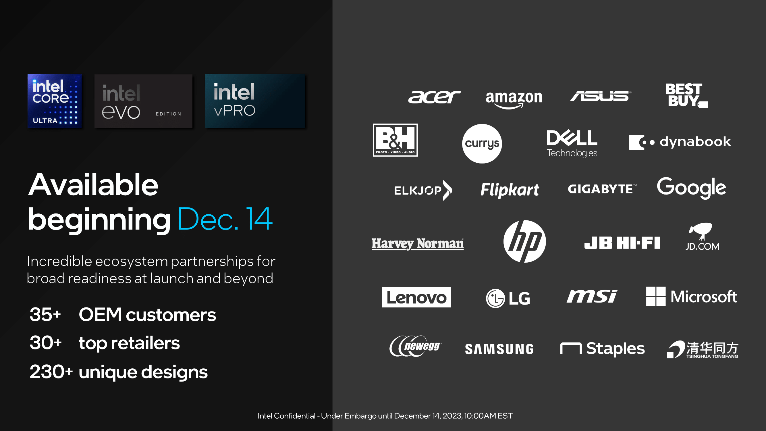
The Intel Core Ultra H and U-series processors are available today, with over 35 OEMs offering different models, including Acer, ASUS, Dell, HP, Lenovo, and MSI. The only SKUs not launching today include the Intel Core Ultra 9 185H, Core Ultra 7 164U, and Core Ultra 5 134U, which are expected to launch sometime in Q1 2024. At the time of writing, no OEMs have reached out to us with models, and pricing on each part remains unknown.